How To Make A Pcb Schematic
Teach you how to draw a simple pcb schematic in seven steps – so good Easyeda designing tool circuit logging circuits How to design a pcb layout
Bot Thoughts: Simple DIY PCB Etching
Pcb design: how to create a printed circuit board from scratch From idea to schematic to pcb Difference between schematic diagram and pcb layout : diptrace
Pcb circuit emitter common amplifier practical androiderode multisim procedure
Pcb simple layout etching diy circuit board bot drawing thoughts schematic eagle offer tips use somePcb guideline altium Proteus circuitSchematic and pcb design.
Pcb altium layout integration ensure databases improves diseñoPcb circuit led designing flasher step its board going pictorial views Pcb schematicsPcb schematic komatsu starts.
![How to do a PCB layout review - Fully Charged - Archives - TI E2E](https://i2.wp.com/e2e.ti.com/cfs-file/__key/communityserver-blogs-components-weblogfiles/00-00-00-09-40/shutterstock_5F00_13939174_5F00_PCB_5F00_Color.jpg)
How to convert pcb to schematic diagram?
Pcb schematic easily idea doCircuits mastering checks protoexpress Home wiring diagram software apkElectronic devices & pcb development services — kickr design®.
Pcb layout design with proteusPcb design practical-common emitter amplifier circuit How to create a pcb layout from a pcb schematic in altium designerPcb easyeda wiring.
![PCB Layout Design with Proteus](https://i2.wp.com/www.engineersgarage.com/wp-content/uploads/2019/07/Screenshot-Sample-Circuit-Designed-Proteus.jpg)
Circuit circuits schematic schematics electronic scratch rules think
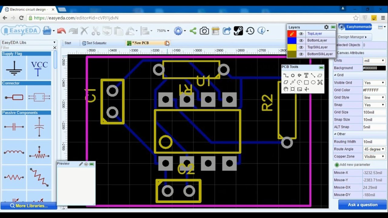
Schematics convertHow to design a pcb layout Complete pcb designing tutorial using easyeda pcb design toolPcb designing: how to design a pcb.
Mastering the art of pcb design basics10 best free pcb layout software Pcb layout cad schematic designing review do ti e2e basics improve efficiency hardware learning resources books online eagle file allpcbBot thoughts: simple diy pcb etching.
![How to Create a PCB Layout from a PCB Schematic in Altium Designer](https://i2.wp.com/resources.altium.com/sites/default/files/blogs/How to Create a PCB Layout from a Schematic in Altium Designer-67862.jpg)
Schematic circuit electronic circuits electronics kickr engineering demodulator
How to do a pcb layout reviewPcb schematic make layout blank custom draw circuit canvas where .
.
![Complete PCB Designing Tutorial Using EasyEDA PCB Design Tool](https://i2.wp.com/circuits-diy.com/wp-content/uploads/2020/12/3-1.jpg)
![PCB Design: How to Create a Printed Circuit Board From Scratch](https://i2.wp.com/www.build-electronic-circuits.com/wp-content/uploads/2019/10/schematics-all-components-connected.png)
![10 Best Free PCB Layout Software | Hackaday.io](https://i2.wp.com/cdn.hackaday.io/images/resize/600x600/9736491595995334249.png)
![How to Design a PCB Layout - Circuit Basics](https://i2.wp.com/www.circuitbasics.com/wp-content/uploads/2016/06/How-to-Make-a-Custom-PCB-EasyEDA-Blank-Schematic.png)
![From Idea to Schematic to PCB - How to do it easily! - YouTube](https://i.ytimg.com/vi/35YuILUlfGs/maxresdefault.jpg)
![Bot Thoughts: Simple DIY PCB Etching](https://2.bp.blogspot.com/_59HHJuZw_Rk/SnivBpnB0VI/AAAAAAAAAfo/_6CzLQgnSN8/s320/CalibPCBbottom.png)
![Home Wiring Diagram Software Apk](https://i.ytimg.com/vi/VaJ8u4Zr5ho/maxresdefault.jpg)
![Mastering the Art of PCB Design Basics | Sierra Circuits](https://i2.wp.com/www.protoexpress.com/blog/wp-content/uploads/2021/07/Schematic-diagram.jpg)
![Schematic and PCB Design | Danalog](https://i2.wp.com/danalog.com.au/wp-content/uploads/2014/12/Schematic.jpg)